

Explore the physical limits at micron and nanometer scales
Semiconductor design
& characterization
From semiconductor power analysis to high-speed digital circuit characterization, we provide measurement solutions tailored to your needs.
Pain Points & Challenges
The measurement challenges
behind semiconductor R&D
Semiconductor R&D pushes against physical limits. Capturing extremely small currents, characterizing ultrafast signal transitions, and evaluating reliability under demanding thermal conditions require precise instruments with a high upfront cost.
Demanding Current Resolution
Measurements may require current resolution in the nanoampere (nA) or even femtoampere (fA) range, making the necessary equipment a significant investment.
High-Voltage Wide-Bandgap Testing
Gallium nitride (GaN) and silicon carbide (SiC) devices require dynamic characterization at high voltages, beyond what many general-purpose instruments can handle.
High-Speed SerDes Validation
Physical-layer characterization of interfaces such as PCIe 5.0 and 6.0 places demanding bandwidth requirements on oscilloscopes.
Pressure on Equipment Budgets
Startup design companies face high initial equipment costs, rapid technology changes, and substantial depreciation.
Recommended Instruments
Instrument categories for
device characterization
Build a high-precision laboratory for device characterization and validation.
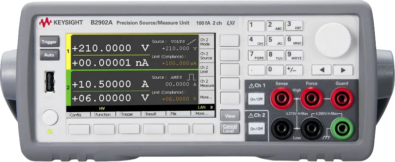
Source Measure Units
Combining power-supply and multimeter functions, SMUs provide high-resolution current–voltage (I–V) measurements at the core of semiconductor device characterization.
Nanoampere-Level Current AccuracyExplore category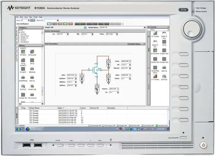
Semiconductor Parameter Analyzers
Multiple plug-in modules support parallel capacitance–voltage (C–V) and pulse characterization for wafer-level testing.
Synchronized Measurement ModesExplore category
High-Bandwidth Digital Oscilloscopes
Perform physical-layer compliance testing on high-speed DDR and PCIe signals to verify signal integrity.
Low Noise Floor, Fast SamplingExplore categoryApplication Case
Semiconductor testing in practice
See how TXRX solutions address real measurement challenges.

GaN Device Characterization
Submicroampere static characterization of GaN power devices
A startup developing gallium nitride (GaN) switching power-supply ICs needed precise measurements of breakdown voltage and leakage current in its power devices.
Using a precision source measure unit (SMU) matrix supplied by TXRX, the customer carried out withstand-voltage testing up to 3,000 V and captured static-current fluctuations at the 10 fA level, helping validate device reliability.
- Up to 3,000 V
- Withstand-voltage testing in this GaN project
- 10 fA
- Static-current fluctuations captured in this project
Scalable Test Support
Scalable testing for rapidly evolving advanced processes
Lower R&D Investment
Reduce the cost of entry for startup research and development teams.
Shorter Equipment Lead Times
Available stock supports immediate laboratory expansion.
Flexible Rental Options
Choose short- or long-term rentals aligned with your project needs.
Expertise Across Brands
Expertise in configuring and coordinating instruments from Keysight, Keithley, and NI.