

Semiconductor Design & Characterization
A structured starting point for planning Semiconductor Design & Characterization measurement requirements.
Challenges this solution addresses
Define the requirement
Document the signal range, bandwidth, channels, interfaces, environment, and intended workflow before selecting equipment.
Review the configuration
Check model options, accessories, software, automation interfaces, and supporting documentation as one configuration.
Plan verification
Confirm calibration, acceptance, logistics, and project timing before a quotation or test plan is finalized.
Connect the workflow
Map fixtures, switching, software, data capture, and operator steps so the complete measurement path can be reviewed.
Recommended instrument categories
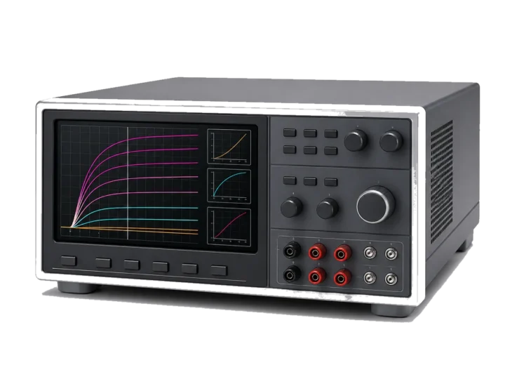
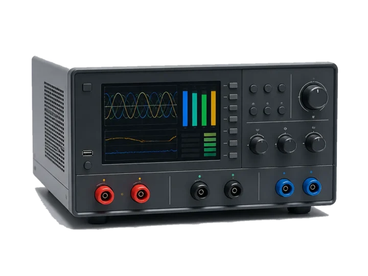
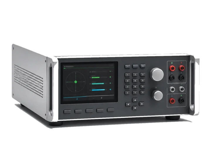
Two ways to apply this solution path
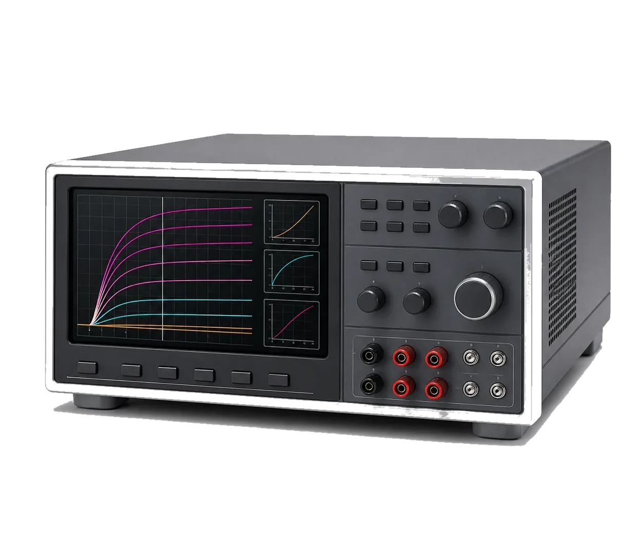
Laboratory setup planning
Translate the range, interfaces, uncertainty target, fixtures, and evidence required for Semiconductor Design & Characterization into an equipment-category shortlist.
Repeatable operational workflow
Review switching, automation, calibration, data capture, and hand-off requirements before the workflow is used for recurring tests.